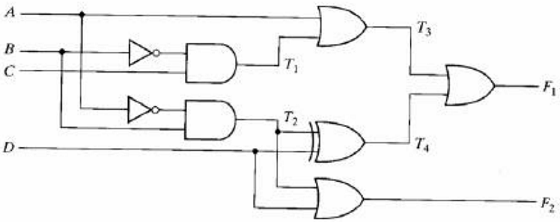
Problem 1: For the following circuit, generate test patterns to test
a. Stuck-at-0 fault at A _________
b. Stuck-at-1 fault at T3 ___________
c. Stuck-at-0 fault at F2____________
Problem 2: For the following circuit, the propagation delay of each XOR gate, AND/OR gate, and clock-to-Q are 6ns, 4ns, and 2ns, respectively. The contamination delays are 4ns, 3ns, and 1ns, respectively. The clock skew is 3ns. The setup time requirement is 5ns and hold time requirement is 4ns. The clock runs at 60 MHz.
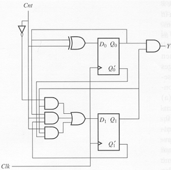
a. Is there any setup time violation? If so, what is the clock frequency that may avoid setup time violation?
b. Is there any hold time violation? If so, what is the clock frequency that may avoid hold time violation?
Problem 3: Draw a transistor level circuit of a 6T SRAM cell, including bit-lines and word-line.
Problem 4: Draw an ESD protection circuit.
Problem 5: Draw CMOS transistors for the two ways to implement the same function, and compare their static and dynamic power:
a. Directly build a complex gate using CMOS transistors: F=(AB(C+D))'
b. Use CMOS transistors to build NAND, NOR and NOT gates, then implement: F=NOT(NOR(NAND(A,B),NOR(C,D)))
You need to size the transistors so that the driving strength of each gate equals a unit inverter, before making the comparison. To estimate the dynamic power, add the total gate capacitance. To estimate the leakage power, consider the resistance of the leakage path.
Problem 6: Answer the following questions:
a. What is the main advantage of flip-chip?
b. Using body-bias, what characteristic of the transistor do we want to change (not power)?
c. If we slow down the clock, do we save power or energy?
d. In a flush memory, where is the information stored? In what form?
e. During buffer insertion, if we have three intermediate solutions before reading the beginning of the circuit: Solution A has delay=100 and capacitance=20; Solution B has delay=200 and capacitance=10; Solution C has delay=200 and capacitance 20. Which solution(s) can be deleted?
Problem 7: Draw a buffered clock tree and specify the position of its root for the following sinks. For every 3-5 sinks, a buffer is needed. To receive any credit, the path from the root to all sinks must be the same distance, and the routing must be rectilinear. To receive full credit, the total wire length of the tree must be minimum.