Discuss the following in detail:
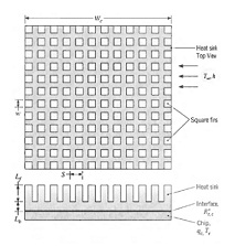
Q: As a means of enhancing heat transfer from high-performance logic chips, it is common to attach a heat sink to the chip surface in order to increase the surface area available for convection heat transfer. Because of the ease with which it may be manufactured (by taking orthogonal saw cuts in a block of material), an attractive option is to use a heat sink consisting of an array of square fins of width w on a side. The spacing between adjoining fins would be determined by the width of the saw blade, with the sum of this spacing and the fin width designated as the fin pitch S. The method by which the heat sink is joined to the chip would determine the interfacial contact resistance, Rt,c.
Consider a square chip of width Wc = 16 mm and conditions for which cooling is provided by a dielectric liquid with T8, = 25°C and h = 1500 W/m2 · K. The heat sink is fabricated from copper (k = 400 W/m · K), and its characteristic dimensions are w = 0.25 mm, S = 0.50 mm, Lf = 6 mm, and Lb = 3 mm. The prescribed values of wand S represent minima imposed by manufacturing constraints and the need to maintain adequate flow in the passages between fins.
(a) If a metallurgical joint provides a contact resistance of Rt,c = 5 X 10⁻⁶ m2 · K/W and the maximum allowable chip temperature is 85°C, what is the maximum allowable chip power dissipation qc? Assume all of the heat to be transferred through the heat sink.
(b) It may be possible to increase the heat dissipation by increasing w, subject to the constraint that (S - w) > 0.25 mm, and/or increasing Lf (subject to manufacturing constraints that Lf < 10="" mm).="" assess="" the="" effect="" of="" such="">