Assignment:
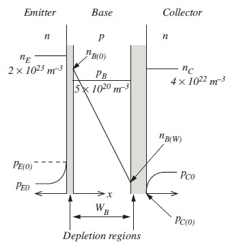
The figure represents the carrier densities in the three neutral regions of the transistor under active conditions. The base-emitter junction is forward-biased by 0.6 volts and the base collector junction is reverse biased by 1 volt.
The biased minority carrier densities are a function of distance x from the junction interface. In the emitter the minority carrier density is represented by pE(x) and at the emitter-base junction interface by pE(0). Similarly, in the base nB(x) is represented by nB(0) at the emitter-base junction interface. The minority carrier density in the collector is pC(x)
The base-region is sufficiently thin (WB << LN, where LN is the electron diffusion length) as to allow us to assume a linear minority gradient dnB(x)/dx
(a) Calculate the values of pE(0), nB(0) and pC(0).
(b) Estimate the collector current density if the width of the base is 1.1 m.
(c) Calculate the minimum cross-sectional area of the base if the transistor is to be capable of carrying 1 ampere and if the base-collector interface is represented by pC(0).