Response to the following problems:
1. A current-mirror-loaded NMOS differential amplifier operates with a bias current I of 200 μA. The NMOS transistors are operated at VOV = 0.2 V and the PMOS devices at /VOV/ =0.3 V. The Early voltages are 20 V for he NMOS and 2 V for the PMOS transistors. Find Gm, Ro, and Ad. For what value of load resistance is the gain reduced by a factor of 2?
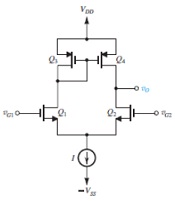
2. This problem investigates the effect of transistor mismatches on the input offset voltage of the current-mirror-loaded MOS differential amplifier of Figure. For this purpose, ground both input terminals and short-circuit the output node to ground.
(a) If the amplifying transistors Q1: and Q2: exhibit a W/L mismatch of ?
VOS1=(Vov/2) Δ(W/L)A/(W/L)A
(W/L)A, find the resulting short-circuit output current and hence show that the corresponding VOS is given by where VOV is the overdrive voltage at which Q1: and Q2: are operating.
(b) Repeat for a mismatch _(W/L)M in the W/L ratios of the mirror transistor Q3: and Q4: to show that the corresponding VOS is given by
VOS2=(Vov/2) Δ(W/L)M/(W/L)M
where VOV is the overdrive voltage at which Q1:and Q2:are operating.
(c) For a circuit in which all transistors are operated at /VOV /* = 0.2 V and all W/L ratios are accurate to within ±1% of nominal, find the worst-case total offset voltage VOS.