Response to the following problem:
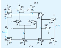
In the CMOS op amp shown in Fig., all MOS devices have /Vt /= 1V, μn Cox =2 μpCox =40 μA/V2, /VA / = 50 V, and L = 5 μm. Device widths are indicated on the diagram as multiples of W, where W = 5 μm.
(a) Design R to provide a 10-μA reference current.
(b) Assuming vO =0 V, as established by external feedback, perform a bias analysis, finding all the labeled node voltages, and VGS and ID for all transistors.
(c) Provide in table form ID, VGS, gm, and ro for all devices.
(d) Calculate the voltage gain vo/ (v+ -v- ) , the input resistance, and the output resistance.
(e) What is the input common-mode range?
(f) What is the output signal range for no load?
(g) For what load resistance connected to ground is the output negative voltage limited to -1 V before Q7:begins to conduct?
(h) For a load resistance one-tenth of that found in (g), what is the output signal swing?