Design of an operational Amplifire using Pspice:
Fig: operational Amplifire using Pspice
1 Learning outcomes
At the end of this lab, you will:
• be able to produce a functioning operational amplifier circuit by combining different stages.
• be aware of problems and challenges to meet a specification for designing and characterising an operational amplifier.
2 Objectives:
It is required to design an operational amplifier with the aid of PSpice software to satisfy the following design specifications:
a) Differential input impedance greater than 100 kQ.
b) Voltage gain (that is, 'open loop gain') greater than 500,000.
c) Output impedance less than 1
d) Output voltage to be approximately zero volts for zero input.
e) Frequency response down to DC (0 Hz).
f) Supply voltage +9 to -9 volts.
g) Total current consumption not greater than 5 mA.
3 Introduction:
This experiment requires you to design and simulate an operational amplifier circuit. A practical integrated circuit version (e.g. a 741 type) would in addition contain a `push pull' output stage and extra components to provide further temperature and supply variation immunity.
Other circuit complications arise due to problems integrating NPN and PNP high gain transistors together on the same chip. The experiment is intended to reinforce lecture material in module ELEC271, and reference to the relevant lecture notes is essential.
3.1 Operational amplifier
An operational amplifier (op-amp) is a high-gain voltage amplifier with a differential input and a single-ended output (Figure 1 (a)). It is among the most widely used electronic devices today, being used in a vast array of consumer, industrial, and scientific devices, with very low cost. The op-amps had their origins in analogue computers where they were used in many linear, non-linear and frequency-dependent circuits. Their popularity in circuit design largely stems from the fact that characteristics of the op-amp circuits with negative feedback (such as their gain) are set by external components with little dependence on temperature changes and manufacturing variations in the op-amp itself. Examples of op-amp circuits are shown in Figure 1 (b) and (c).
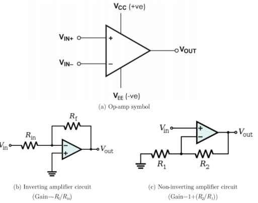
Fig: Operational amplifier and circuit applications
The op-amp is one type of a differential amplifier. Other types of differential amplifiers include the fully differential amplifer (similar to the op-amp, but with two outputs), the instrumentation amplifier (usually built from three op-amps), the isolation amplifier (similar to the instrumentation amplifier, but with added tolerance to common-mode voltages that would destroy an ordinary op-amp), and negative feedback amplifier (usually built from one or more op-amps and a resistive feedback network).
3.2 The design The op-amp you are required to design can be constructed from four basic 'building block' circuits:
a) An emitter follower
b) A common emitter amplifier
c) A current mirror circuit
d) A differential input stage (long-tailed pair)
The designed operational amplifier schematic will be simulated using PSpice software library models located in the EVAL library using the following devices:
• Q2N2222 NPN transistor
• Q2N2907 PNP transistor
The output from your differential amplifier should be fed into the input of the common emitter stage. It is also necessary to include an emitter follower circuit as a buffer between the two amplifier stagers. Figure 2 shows a block diagram of the op-amp.
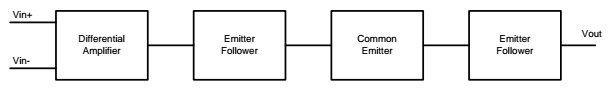
Fig: Block diagram of the op-amp
The properties of these blocks should have been investigated and design procedures established in the exercise 'Pre-lab Test for Experiment 5'. It is essential that this is done before commencing.
4 Experimental work:
4.1 Part I: Transistor output characteristics
Objective: To obtain a set of output characteristics for the two transistor types to be used in this experiment.
Obtain a plot of the output characteristics of the 2N222 transistor, i.e. IC vs. VCE (0 to 20 V in steps of 0.5 V) for a range of IB (0 to 40 μA in steps of 4 μA).
Procedure:
• Task-1: Input the circuit schematic of Figure 3 in PSpice schematics.
• Task-2: In the 'Analysis' menu, select 'Setup.? and check the 'DC sweep' option and input the variable as lice' with the desired range. Click on 'Nested sweep' option to set the base current IB steps. Thus, for each value of IB (0, 4, 8 40 μA), VCE is swept from 0 to 20 V.
• Task-3: Close the 'Analysis setup' window. In the 'Analysis' menu, select `Simulate' (you can do that by pressing on F11 key as well). A response curve will appear. Take a screenshot of this response.
• Task-4: From the curve, estimate the DC current gain, β (also known as hFE) at Ic˜2 mA. Estimate also the AC (small signal) current gain, βo(also known as hfr) . Hint: see your notes on how to do this. Record your results.
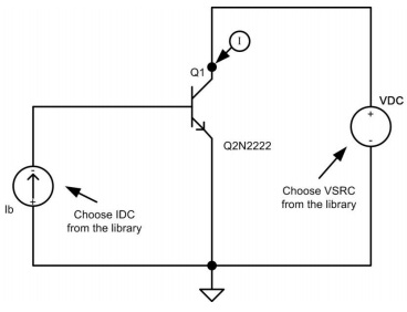
Fig: Transistor output characteristics
4.2 Part II:
Achieving the specification of the operational amplifier
Objective: To build the complete operational amplifier circuit and obtain the required specification.
Start now building the complete circuit of the operational amplifier (see the given `tutorial' lecture for ELEC271 on VITAL).
Procedure:
• Task-1: Combine the required stages to build a complete operational amplifier in PSpice.
• Task-2: Obtain the transfer characteristics of your amplifier by grounding one input and performing a DC sweep from -9V to +91.1 on the other input. Identify the useful operating range from your plot. You will need to narrow the sweep range to achieve an accurate useful range.
• Task-3: Find the open loop gain (Ad) of the amplifier from the useful range in the above step.
• Task-4: Determine the required DC voltage offset from the transfer characteristic. Use this value to help balance the amplifier - you can apply a small DC offset to one of the inputs to try to centre the output close to zero volts.
• Task-5: Obtain a set of input/output waveforms (in useful range) from a transient simulation, and from which, calculate the gain of the amplifier. Verify that the specification has been met. Record your results.
• Task-6: Obtain a set of input waveforms (in useful range) in an AC sweep simulation, add an input impedance trace and calculate the average value of it. Change the trace and calculate the average output impedance. Hint: The screenshots of the corresponding impedance (V//) should be taken — the impedance values can be found in the bandwidth.
• Task-7: Display the currents and voltages on the schematic and watch out the DC voltage levels and total current consumption.
4.3 Part III: Obtaining the frequency response of the designed amplifier Objective:
To obtain the gain and phase Bode plots of the designed amplifier.
Now, obtain the frequency response of the designed amplifier by determining the gain and phase Bode plots.
Procedure: • Task-I: Determine Bode plots (gain and phase) of your amplifier by replacing the VSIN input sources with VAC parts in PSpice and run an AC sweep. The parameters of the VAC part should be set to match those used in your VSIN part. Take screenshots of the Bode plots.
• Task-2: Add phase compensating capacitor (say 30 pF or any suitable value) between the collector of the common emitter stage and the base of the lust emitter follower. Investigate the effect on the Bode plots. Take screenshots and record your findings.
5 General questions:
a) What can you deduce about the stability of your amplifier from the Bode plots in Part III?
b) What is the purpose of the 'Phase compensating capacitor'?
6 Report writing guidelines for Experiment 5
• This experiment is assessed by means of a formal report. Use the formal report template (available on VITAL) to write your report. The idea behind this report is to document your experience and technical findings in this experiment.
• In your 'Results' section, include the following: All your findings and measurements along with all the screenshots of schematics and simulations. Make sure to comment on each result and simulation. - The table shown overleaf (Table I) with your own results. Make sure to write relevant comments in the fourth column.
• In your 'Discussions and Conclusions' section include the following:
- Describe any problems you have experienced while carrying out both experiments and explain your problem-solving methods that you have followed.
- Include the answers to the general questions (Section 5 above).
- Does your designed op-amp achieve the specification> If not, explain the reasons.
• Important: make sure that all your figures (scematics and simulations) are clear and all the numbers on the figures and readable.
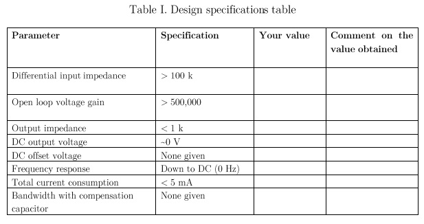
Fig: Design specifications table