Introduction:
The goal of this project is to design a BJT amplifier with a gain of -10, an input resistance of 1kΩ and an output resistance of 3.3kΩ that satisfies the schematics depicted in figure.
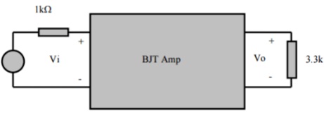
Note that the source resistance matches the input resistance of 1kΩ. Likewise, the load resistor matches the output resistance of 3.3kΩ. Since the gain desired is -10, an implied specification is that the BJT topology required will be an NPN common emitter amplifier.
Part I:
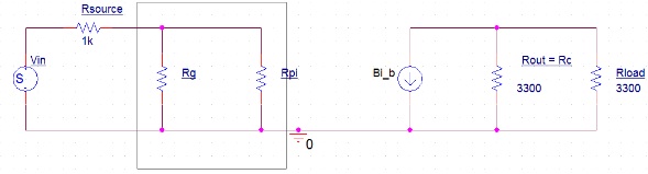
1. Build the common emitter model used in AC small signal analysis and set the value of the input and output resistances.
2. Match the source resistor to the input resistance and the load resistor to the output resistance as per illustration 1.
3. Derive the gain equation for the circuit.
4. The next step was to solve for ICQ by solving for Rπ and substituting the result into the gain equation.
5. The next step is to solve for β using the relationship in step 4, by taking Rπ to equal the input resistance
6. With β and ICQ known, solve for Rπ using the relationship in step 4.
7. IBQ was then found by dividing ICQ by β.
8. The relationship of Rin to Rb and Rπ was used to calculate Rb.
9. Find RE, using the following relationship.
RE = 10 (RB/1 + β)
Part II:
1. Generate the DC small signal analysis model to find the remaining component values.
2. Find VBB using the following equation
VBB = .7 + IBQ(RB + (RE * (1 + β)))
3. Find VCC using the following equation
VCC = (ICQ)(RAC + RDC)
4. Find R1 and R2 using the following relationships:
VBB = (VCC) [R2/(R1+R2)]
1000 = R1R2/(R1+R2)
Part III:
1. Construct and simulate the circuit in pSpice software so that the calculated values could be tested. Note that the transistor beta value was set to 20 and the input signal was a sinusoid of .001 v amplitude at 1kHz frequency (See results)
2. Create and run a new simulation profile capturing the input and output waveform across 25 ms.
3. Visually determine whether or not a gain of -10 was achieved.