Post All assignments separately.
Assignment 1:
Answer Question one and any three other questions
1.
a) Draw the equivalent circuit of a bipolar transistor at mid-frequencies. Explain briefly the physical meaning of each component, rb’e , rbb’, rce and βo.
b) Sketch a typical frequency response of a common-emitter voltage amplifier and explain its form.
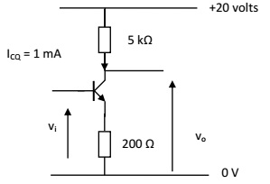
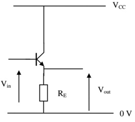
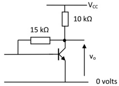
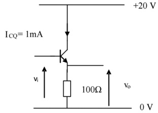
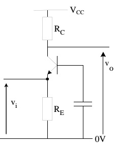
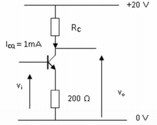
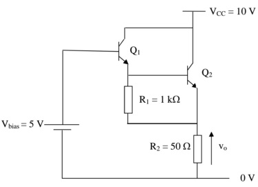
c) The figure below shows a transistor amplifier circuit in which the quiescent DC collector current is 1 mA. Assuming that rce may be neglected, calculate the voltage gain vo/vi. What is the application for this circuit?
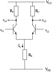
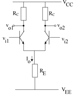
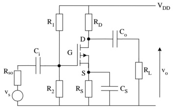
d) The figure below shows a differential amplifier. Derive the ac equivalent circuit for the common-mode gain and hence derive an expression for it.
e) Negative feedback allows engineers to construct precision amplifiers. Explain what is meant by precision in this context and why negative feedback allows the achievement of precision performance.
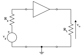
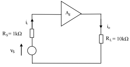
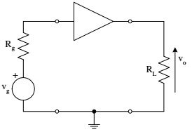
f) The triangular element in the circuit shown in the figure below represents an ideal current amplifier with a gain of 100. Work out the value of the voltage gain if Rg = 5 kΩ and RL = 10 kΩ.
g) Explain what is meant by the term ‘virtual short principle’, in relation to operational amplifiers.
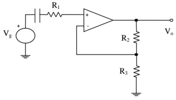
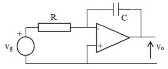
h) An operational amplifier circuit is shown below. The op-amp is constructed using bipolar transistors. Explain why the circuit would not work. Suggest another way of achieving a low frequency roll-off.
i) Explain what is meant by ‘slew rate’ in relation to an operational amplifier and the effect that it has on performance. How would you avoid its effect in a design?
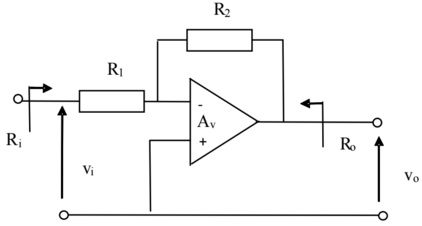
j) Identify the feedback topology of the circuit below. What amplifier property is stabilised? Use feedback theory to estimate the voltage gain.
2.
a) You are required to design a 2-stage voltage amplifier (find values for RE and RC2) to meet the following criteria: an input resistance of at least 100 kΩ and an overall voltage gain greater than 100, with a resistor output load of 20 kΩ. Use a common-collector (emitter-follower) stage for the input and a common-emitter stage, both biased at 0.5 mA.
VCC = 20 V, βo = 160 and the DC level of the common-emitter stage needs to be set at half the supply voltage. Proceed as follows:
i) Draw a schematic circuit of your amplifier, omitting the bias resistors.
ii) Find the value of the collector resistor of the second stage and hence its gain.
iii) Consider the input resistance and find the value of RE.
iv) Work out the gain of the first stage and hence the total gain. Check that it meets the criterion.
b) Suggest ways you could increase the gain and the input resistance
3.
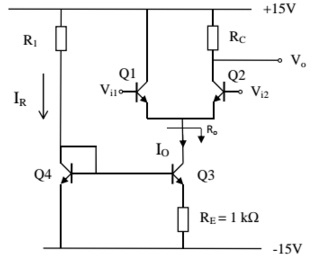
a) The figure below shows a Widlar current mirror.
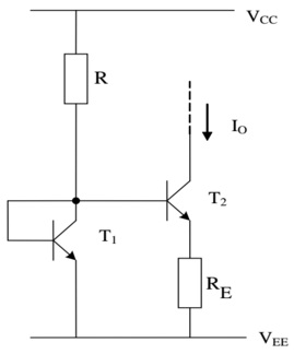
i) Neglecting base currents and assuming T1 and T2 are identical transistors, show that the current Io, is given by:
IoRE = VT ln(IR/Io)
where VT = kT/q; the other symbols have their usual meanings.
ii) The current mirror is required to provide the bias for a differential amplifier with resistor loads, RC1 = RC2 = RC. Sketch amplifier circuit in your answer book. Design the circuit (calculate all resistor values) to give a DC bias current (in T2 above) of 0.1 mA and a DC output voltage of the differential amplifier of V0 = 0 V.
VCC = 10 V, VEE = -10 V. Hint: allow 4VT across RE.
iii) Draw the ac small-signal equivalent circuit of the amplifier and hence estimate the differential voltage gain. Explain any approximations and assumptions used in your calculations.
b) Do you expect that the amplifier will have a large or small common-mode rejection ratio? Explain your reasoning.
4.
a) For the common emitter amplifier equivalent circuit shown below, apply Miller’s Theorem and hence show that the input impedance is given by:
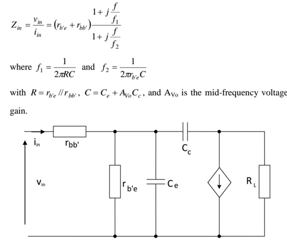
b) Show that Zin reduces to:
Zin ~ (rb'e + rbb) at low frequencies such that f << f1, f2
Zin ~ bb' at high frequencies such that f >> f1, f2
Can the amplifier be used at frequencies f >> f1, f2?
c) Sketch Zin (f). labelling your diagram appropriately, for the case of β0 = 200, rbb’ = 100 Ω, a bias current of 1 mA, load resistor of 2 kΩ, Ce = 10 pF and Cc = 2 pF.
5.
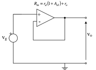
a) The figure below shows an operational amplifier circuit.
i) Identify the feedback topology and hence the amplification property that is stabilised by the feedback. What is the gain of the amplifier?
ii) Sketch the equivalent circuit of the amplifier and show that the loop gain, T of the amplifier is given by the expression:
T = Aol [rd/(ro + rd)]
Where rd, ro are the differential input resistance and output resistance respectively and Aol is the open loop gain of the ampifier.
b) Using the expression above,
i) Calculate a value for T.
rd = 10 kΩ, ro = 100 Ω, Aol = 105
ii) Hence estimate the input and output resistance of the amplifier. 2
iii) Suggest some applications for this amplifier circuit. 2
6.
a) List the advantages and disadvantages for the use of negative feedback in electronic systems
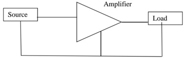
b) Draw a block diagram of an amplifier with feedback, labelling clearly the open loop gain Aol and feedback fraction, β. Show that the gain with feedback is given by:
Af = Aol/(1 + Aolβ)
Under what conditions is the closed loop gain insensitive to variations in the open loop gain?
c) The figure below shows an amplifier with feedback.
i) Identify the feedback topology and hence the amplifier type. 4
ii) Represent the circuit as a negative feedback system and hence estimate the appropriate gain. State any approximations used in your analysis
Assignment 2:
Answer question one AND any other three questions.
1.
a) Explain what is meant by the term ‘small signal equivalent circuit’. How is it used in electronics design?
b) Fig shows a transistor amplifier circuit in which the quiescent DC collector current is 1 mA. Assuming that rce may be neglected, calculate the voltage gain vo/vi. What is the application for this circuit?
c) Figure shows a differential amplifier. Derive the ac equivalent circuit for the differential mode gain and hence derive an expression for it.
d) Draw the ac equivalent circuit of a MOSFET device and hence show that the gain-bandwidth product is given approximately, by fT = gm/2ΠC, where gm, is the transconductance and C is the sum of gate-source and drain source capacitance. State any approximations employed.
e) Explain physically, the Miller Effect. How does it influence amplifier performance? Suggest a circuit configuration that does not suffer from Miller Effect and explain why.
f) Figure shows an ideal transconductance amplifier with a gain of 10 μA/V connected to a load resistor RL = 10 kΩ. Calculate the voltage gain vo/vi of the circuit.
g) Figure shows an inverting operational amplifier circuit. Identify the feedback topology used in the circuit. Describe briefly the effect that the feedback will have on the input resistance Ri and output resistance Ro of the circuit.
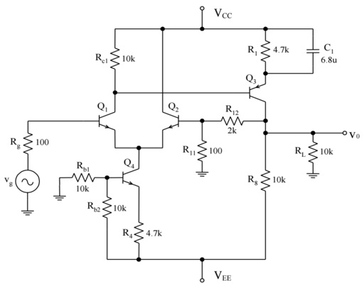
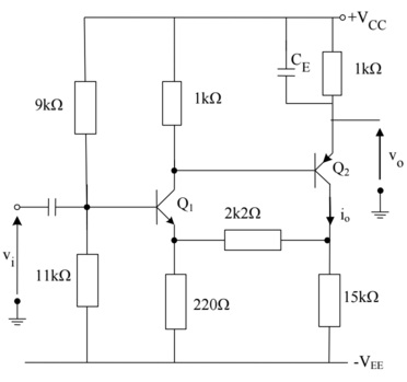
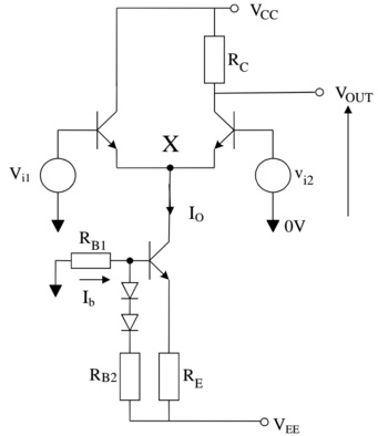
The following questions (h-j) apply to Figure. VCC = 10V, VEE = -10V and β = 100 for all transistors.
State and explain carefully all approximations used in your calculations.
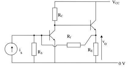
h) What is the voltage at the base of transistor Q4 and hence what is the collector current of Q4?
i) Estimate the voltage at the collector of transistor Q1 and hence the collector current of transistor Q3. What is the function of the circuit block represented by transistors Q1, Q2?
j) Identify and describe the forward path of the signal through the amplifier from the source to the load, and determine the path taken by the feedback signal. What types of output sensing and input summing are being used in this amplifier circuit?
2.
a) You are required to design a 2-stage voltage amplifier (find values for RE, RC1, RC2) to meet the following criteria: an input resistance of 100 kΩ and an overall voltage gain greater than 500, with a resistor output load of 10 kΩ. Use a common-emitter with emitter degradation (RE) stage for the input and a common-emitter stage biased at 1mA.
(VCC = 20V, βo = 250 and the DC level of the first stage output needs to be set at half the supply voltage. Allow 10% of VCC across RE). Proceed as follows:
i) Draw a schematic circuit of your amplifier, omitting the bias resistors.
ii) Work out the bias current and emitter resistor value to meet the input specification. Hence find the value of the collector resistor of the first stage.
iii) Work out the gain of the first stage and hence find the required gain of the 2nd stage.
b) Comment on the ‘quality’ of your voltage amplifier and suggest how it could be improved.
3.
a) Figure shows the circuit of a basic operational amplifier made up of individual stages that have been identified as 1 to 5. Briefly describe the purpose of each of these stages.
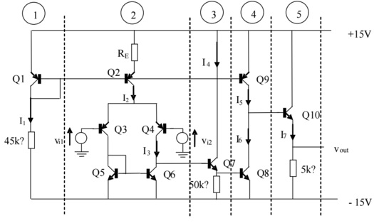
b) If I2 = 0.2 mA, make reasonable approximations to estimate the total current drawn by the circuit from the ±15V DC voltage supply when the amplifier is biased so that the DC value of Vout = 0 V and the ac input signals are zero.
c) Assuming that the voltage gains of the two common collector stages 3 and 5 are both unity, make reasonable approximations to estimate the overall small signal voltage gain of the amplifier, Av, where:
AV = Vout/Vi1 - Vi2
Assume that all the transistors have a current gain of 100 and an Early voltage of VA = -100 V.
4.
a) Figure shows a common-source amplifier. Construct the ac equivalent circuit, then apply Miller’s Theorem and hence show that the voltage gain is given as:
AVS = -gmRt [1/{1 + j(f/fH)}]
Where fH = 1/2πRSC is the voltage gain bandwidth.
Rt = RD || RL and C = [Cgs + (1 + gmRt)Cgd]
State clearly any approximations or assumptions used in your analysis.
The parameters above are defined as follows: gm is the transistor transconductance, Cgs and Cgd are the internal capacitances between the gate/source and gate/drain respectively.
[Assume that the capacitors C1, C2, C3 are short circuit at the frequencies of interest and that the bias resistors R1, R2 are large.]
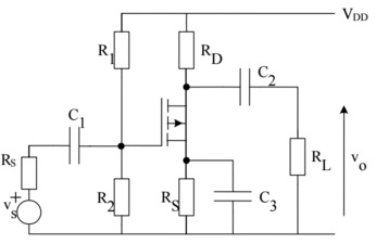
b) Sketch the gain as a function of frequency and indicate clearly the bandwidth, fH and the mid-frequency gain region.
c) Your amplifier is to be used with a transducer with a high internal resistance, RS = 100 kΩ. Design the amplifier (chose the value of dc bias current, ID) to give a mid-frequency gain of -10.
Cgs = 4pF, Cgd = 1pF, Rt = 22 kΩ and the drive constant of the MOSFET, β = 0.1 mA/V2
For the MOSFET in saturation, gm = √2I Dβ .
d) Hence work out the bandwidth
Justify any approximations used in the analysis.
5.
a) Figure shows an inverting amplifier system. Using the virtual short principle, work out the voltage gain, vo/vi if Rf = 10 kΩ and R = 1 kΩ. Identify the form of the output sampling and input summing and so identify the amplifier type.
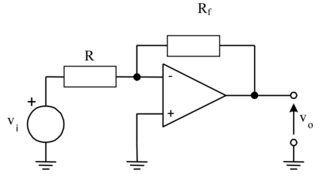
b) Draw an equivalent circuit for the amplifier system and hence show that the resistance looking into the inverting input of the operational amplifier may be estimated as:
Ri = rd ||(Rf/1 + Aol)
where rd is the differential input resistance of the operational amplifier and Aol is its open-loop gain.
c) Estimate Ri if Aol = 105 and rd = 100 kΩ. Comment on the value obtained.
d) Draw a schematic diagram to indicate how you would analyse the circuit to find the amplifier output resistance. Would you expect the value to be large or small?
6.
a) List the advantages and disadvantages of using negative feedback in electronic systems.
b) Draw a block diagram of an amplifier with feedback, labelling clearly the open loop gain Aol and feedback fraction, β. Show that the gain with feedback is given by
Af = Aol/(1 + Aolβ)
Under what conditions is the closed loop gain insensitive to variations in the open loop gain?
c) Identify the feedback topology of the amplifier shown in figure and hence the amplifier type. Represent the circuit as a negative feedback system and hence estimate the appropriate gain.
State approximations used in your analysis.
Assignment 3: Answer Question 1 and any three other questions.
1.
a) Draw small-signal ac equivalent circuits of bipolar and MOSFET transistors at mid-frequencies. Compare and contrast the ac parameters for transconductance and output resistance for applications in analogue circuits.
b) Sketch a typical frequency response curve (AV versus f ) of an ac-coupled common-emitter voltage amplifier. Explain the form of the curve, indicating clearly the reasons for the low and high frequency roll-off.
c) Figure below shows a transistor amplifier circuit in which the quiescent DC collector current is 1mA (the bias resistors are omitted). Assuming that rce and RE are large enough to be neglected, draw the equivalent circuit and calculate the voltage gain, vo/vi. State an application for this amplifier. The collector resistor, RC = 2 kΩ.
d) Figure below shows a simplified diagram of a cascode amplifier. Consider it as a two-stage amplifier and hence show the voltage gain is approximately given by AV = -gm x RC
What is the main application for this amplifier?
e) The triangular element in the circuit shown in the figure below represents an ideal trans-resistance amplifier with a gain of 100 kΩ. Work out the value of the voltage gain, vo/vg if Rg = 5 kΩ and RL = 10 kΩ.
f) Figure shows a switched capacitor circuit with a two-phase clock, φ1, φ2 applied.
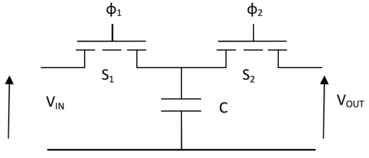
Explain briefly the circuit operation and hence show that it represents resistance, Req
Req = 1/fcl x C
Where fcl is the clock frequency.
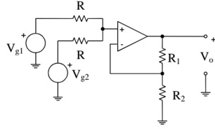
g) The op-amp shown in Figure is ideal. For the condition R1 = R2, show that the output voltage, Vo is given by Vo =Vg1 + Vg2
How would you modify the circuit to obtain a gain of 10? State all assumptions used in your analysis.
h) Explain the meaning of the terms, ‘voltage offset’ and ‘offset current’, in relation to operational amplifiers. How would you alleviate these problems for the case of the inverting operational amplifier circuit?
2. You are required to design a common emitter voltage amplifier (find values for the resistors) to meet the following criteria: a collector current of IC = 1 mA, DC voltage rail, VCC = 10 V and VBE(on) = 0.6 V.
a) Sketch the schematic circuit and calculate the four resistor values, RC, RE, RB1 and RB2 to meet the required specification, according to the following guidelines:
i) Allow 0.1× VCC across RE,
ii) about 0.5 VCC at the collector node,
iii) the current in the base bias resistors should be ten times greater than the DC base current, where the DC current gain is 200.
Comment on each guideline.
b) The voltage gain of your amplifier is required to be greater than 50. Write down an expression for the voltage gain (see attached Amplifier Properties) and hence find the minimum value of load resistor, RL that could be used, to satisfy this requirement.
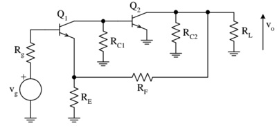
3. Figure below shows a differential amplifier with current source biasing.
a) Explain the good features of this design.
b) Design the circuit (estimate values for the resistors) to meet the following
specification: IO = 1 mA and the DC level at VOUT = 0 V.
(Allow 2 V across RE, the current in the bias circuit, Ib = 0.1× IO and a forward-bias diode drop is 0.6 V. You may assume ideal transistors with high DC current gain.
VCC = 10 V, VEE = −10 V.)
c) Explain why point ‘X’ can be considered an ac ground for differential signals and hence draw an ac equivalent circuit for the differential amplifier. Use the equivalent circuit to estimate the differential gain.
4. Figure shows a common-source amplifier.
a) Construct the ac equivalent circuit. Apply Miller’s Theorem and hence show that the mid to high frequency voltage gain is given as:
AVS = -gmRt 1/[1 + j(f/fH)]
where fH = 1/(2Π x RSoC) defines the high frequency roll-off
Rt = RD||RL and C = [Cgs + (1 + gmRt)Cgd]
State clearly any approximations or assumptions used in your analysis. The parameters above are defined as follows: gm is the transistor transconductance, Cgs and Cgd are the internal capacitances between the gate/source and gate/drain respectively.
You may assume that the capacitors Cb Co CS are short circuit at the frequencies of interest and that the bias resistors R1, R2 are large compared to Rso.
b) Calculate a value for fH.
Parameters have the following values: Rt = 10 kΩ, bias current ID = 1 mA, the drive constant of the MOST, β = 1 mA/V2, gm = √(2 x ID x β), Cgs = Cgd = 0.5 pF and RSo = 10 kΩ
c) The low-frequency roll-off is to be set by the capacitor CS. Design the amplifier to have a low-frequency roll-off, fL = 100 Hz.
You may assume that RS is much greater than the impedance of CS at the frequency of 100 Hz.
5. Figure below shows an operational amplifier circuit.
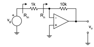
a) Identify the feedback topology and hence the amplification property that is stabilised by the feedback. Work out the voltage gain of the amplifier assuming an ideal op-amp.
b) Sketch the equivalent circuit and hence work out a value for the loop gain, T of the amplifier for the following op-amp parameter values: differential input resistance, rd = 10 kΩ, output resistance, ro = 1 kΩ and open-loop gain, Aol = 103
c) Work out the input (Rn in Figure) and output resistance. Is this a good op-amp? Explain your reasoning.
6.
a) List the advantages and disadvantages for the use of negative feedback in electronic systems.
b) Draw a block diagram of an amplifier with feedback, labelling clearly the open loop gain Aol and feedback fraction, β. Show that the gain with feedback is given by
Af = Aol/(1 + Aolβ)
Under what conditions is the closed loop gain insensitive to variations in the open loop gain?
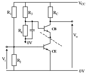
c) Figure below shows the circuit of an amplifier with feedback, partially prepared for a.c. analysis by removing the large bias resistors and coupling capacitors and shorting out the DC supply.
i) Identify the feedback topology and hence the amplifier type.
ii) Represent the circuit as a negative feedback system and hence estimate the appropriate gain, assuming that the open-loop gain of the amplifier is large. State the approximations used in your analysis.
RF = 25 kΩ, RE = 2.2 kΩ.
Assignment 4:
Answer ALL Questions.
1.
a) Draw the small-signal equivalent circuit for a bipolar transistor, labelling clearly the parameters. Work out values for the parameters, gm, rce and rbe (the parameters have their usual meaning). The DC collector current is 1 mA; ac current gain, βo is 100 and the Early voltage, VA is 100 V.
b) Figure shows an amplifier circuit where bias resistors are omitted. Identify the amplifier type and hence design it to have a voltage gain of 10.
c) Figure shows an amplifier system. The source has a high internal impedance and the load is a large resistance. Choose a suitable amplifier type to ensure good matching between source and load. Hence sketch a systems diagram with appropriate equivalent circuits for the source (Thevenin or Norton) and generic amplifier type.
d) Work out the dc voltage levels of the circuit of Fig. and hence find values for IC(Q1), IC(Q2), IR1, IR2. VBE (on) = 0.6 V and dc base currents can be assumed negligible.
e) Draw the ac equivalent circuit of a MOSFET common source amplifier at high frequency. Hence derive an expression for the gain-bandwidth product, fT. State any assumptions made.
f) State the advantages and disadvantages of negative feedback.
g) Design the operational amplifier circuit of Figure to have an input resistance of 10 kΩ and a time constant (R × C) of 10 μs. What function does the circuit perform?
h) Figure shows a schematic diagram of a feedback amplifier with bias components removed. Identify the feedback topology and the amplifier type. Hence write down an expression for the feedback fraction, β.
2.
a) Perform a simple initial design of an ac coupled common-emitter amplifier with four resistor biasing and emitter by-pass capacitor, to have a voltage gain of about 100, for the following conditions. Justify any approximations used.
i) Transistor ac common-emitter gain, βo = 100
ii) Supply voltage of VCC = 20 V
iii) Allow 10% VCC across RE
iv) DC collector voltage of 10 V
v) DC current in the base bias resistors should be ten times greater than the DC base current.
Assume VBE(on) = 0.6 V. The load resistor, RL = 1 k Ω. (Hint: first find a value for the collector resistor.)
b) Estimate a value for the input capacitor, CIN to set the low-frequency roll-off to be 1 kHz.
c) Which is the preferred way to set the low-frequency roll-off and how is this generally accomplished? What would be a practical value for CIN ?
d) What would be the next step in the design process?
3. Figure shows a differential amplifier where the transistors can be considered to be identical. The voltage gain is given by AV = (gm/2) x RC, VBE (on) ˜ 0.6 V anf VT = 25 mV.
a) Prove the relationship:
RE = (VT/IO) x ln (IR/Io)
and hence design the amplifier (estimate values for resistors R1 and RC ) to give a voltage gain > 100 and a DC voltage level at the output of 0 V . What is the differential input resistance of the amplifier?
b) Explain the meaning of the term ‘common-mode rejection ratio (CMRR)’. Comment on the dynamic resistance (RO) looking into the current mirror and explain its significance for the CMRR.
c) Suggest how the design might be improved to make a better voltage amplifier.
4.
a) Draw a diagram of a negative feedback system. Hence derive the expression for the gain of a negative feedback amplifier, Af in the form:
Af = (1/β)(T/1+T)
Where T = Aolβ , is the loop gain.
b) Draw an appropriate equivalent circuit for the amplifier shown in Figure, and hence derive the following expression for the input impedance.
c) Derive the following expression for the loop gain of the amplifier.
T = Aol (rd/ro + rd)
Estimate values for T, β, Rin and comment on the values obtained. Parameter values are rd = 10 kΩ, ro = 50 Ω and Aol = 105