Response to the following problem:
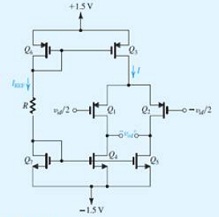
Figure shows a circuit for a differential amplifier with an active load. Here Q1:and Q2: form the differential pair, while the current source transistors Q4: and Q5: form the active loads for Q1: and Q2: respectively. The dc bias circuit that establishes an appropriate dc voltage at the drains of Q1: and Q2: is not shown. It is required to design the circuit to meet the following specifications:
(a) Differential gain Ad =50 V/V.
(b) IREF =I = 200 μA.
(c) The dc oltage at the gates of Q6: and Q3: is +0.8 V. d) The dc voltage at the gates of Q7: Q4: and Q5: is -0.8 V. The technology available is specified as follows: μnCox = 2.5μpCox =250 μA/V2;Vtn =/Vtp /=0.5 V,Van = / VAp /=10 V. Specify the required value of R and the W/L ratios for all transistors. Also specify ID and / VGS _/at which each transistor is operating. For dc bias calculations you may neglect channel-length modulation.