Response to the following problem:
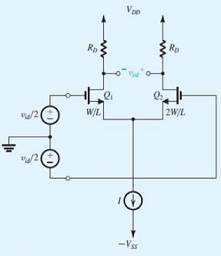
A design error has resulted in a gross mismatch in the circuit of Figure. Specifically, Q2: has twice the W/L ratio of Q1: If vid is a small sine-wave signal, find:
(a) ID1 and ID2.
(b) VOV for each of Q1: and Q2:
(c) The differential gain Ad in terms of RD, I, and VOV Now design the amplifier to obtain a differential gain of 500 V/V. Use /VOV /= 0.2 V. If V1A /= 5 V/μm, specify the required channel length L. If gm is to be as high as possible but the power dissipation in the amplifier (in equilibrium) is to be limited to 0.5 mW, what bias current I would you use? Let VDD = VSS = 0.9 V.