Assignment Introduction:
The primary objective of this practical is to ensure that you have understood the material studied in the theoretical component of the course and to enable you an opportunity to use that knowledge to completely design, simulate, construct and test an actual low-noise, small-signal, high-frequency amplifier.
Design Specification:
The data sheet for the BFP196 BJT is provided. Design, simulate, construct and test a low-noise amplifier (LNA) for the Industrial, Scientific and Medical (ISM) band that will conform to the following specifications:
- Design Frequency: 900 MHz
- Active device bias point: VCE = 8v, Ic = 50mA
- Maximum noise figure: 1.3 dB at 900 MHz
- Minimum gain: 12 dB at 900 MHz
- System characteristic impedance: 50 ohm
- Supply voltage: 12v
The active device should be made unconditionally stable, using the technique of collector shunt stabilization, before implementing the impedance matching networks. The circuit topology should be consistent with a minimum component count and the impedance matching networks implemented with lumped elements.
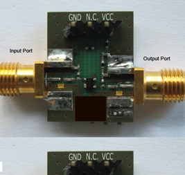
Here is an example of an RF PCB. All designs should look somehow like this.
Requirements:
Problem 1: The design procedure must be completely and clearly documented. A hardcopy of all relevant design data is to be submitted. This should include stability factor data, gain and reflection coefficient data etc. Smith charts showing stability circles, gain circles and noise-figure circles are to be provided. These can be obtained using the circles utility option available with the Ansoft Designer Student Version (SV) Version 2.2.0 or AWR Microwave Office.
Problem 2: A hardcopy of the actual PCB is to be submitted showing all resistor bias network calculations, as well as any RF choke and coupling/decoupling capacitor calculations. Please label all connections.
Problem 3: A neat sketch showing the complete schematic is to be submitted. This should include all bias circuitry as well as any RF choke and coupling/de- coupling circuitry. All component values are to be given, and they must be practical values.
Problem 4: A hardcopy plot is to be submitted, showing the final simulated results of the magnitudes (in dB) of S11, S22, S21 and noise figure. These results are to be plotted over the frequency range from 300 MHz to 1000MHz.
Problem 5: A hardcopy listing of the final circuit simulation file used to produce the plots in 3.4 is to be submitted. The simulation file should include any RF choke circuitry and capacitor coupling/de-coupling circuitry, but it is not necessary to include the dc biasing circuitry.
- Marks will be awarded for innovative design resulting in the best result being
- achieved with a minimum component count.
- Marks will be deducted for sloppy and/or untidy work.
- The PCB should comply with radio frequency design rules (double sided with a solid ground plane on one side and vias if possible). Varyboard artworks will receive zero mark. Surface mounted component should be used Not Leaded Components.
Stuck with Assignment Dilemmas? Low-Noise Amplifier Assignment Help Service Will Sort All Your Academic Woes In No Time!
Tags: Low-Noise Amplifier Assignment Help, Low-Noise Amplifier Homework Help, Low-Noise Amplifier Coursework, Low-Noise Amplifier Solved Assignments, Microwave Engineering Assignment Help, Microwave Engineering Homework Help