Problem 1:
Figure depicts a block diagram of the front end of a communication receiver. The noise characteristics of the critical receiver components are as follows:
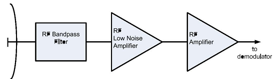
Antenna noise temperature 29 K
RF Bandpass filter passband loss 0.2 dB, physical temperature 30 Co
Low Noise Amplifier gain 25 dB, noise figure 0.5 dB
RF Amplifier gain 23 dB, noise figur 3.3 dB
The noise performance of subsequent components should have virtually no effect on the overall noise performance. Therefore, these details are not specified.
Calculate:
(a) (i) The overall noise temperature of the receiver
(ii) The overall noise factor
(iii) The overall noise figure in dB
(iv) The system noise temperature
(b) If the receiver equivalent noise bandwidth is 65 MHz, and the signal to strength at the antenna connection to the RF band pass filter is 7pW (710-12W), calculate the signal to noise ratio in dB at the receiver output to the demodulator.
Problem 2:
Each student will use a unique sequence of 8 dibits. The sequence is generated by converting the last 5 digits of the student ID into a binary format. If the 5 digit number is larger than 65536 this will lead to more than 16 bits. In this case additional leading bits should be ignored. The windows calculator or the "dec2bin('ID',16)" function in MATLAB, can be used to do the conversion.
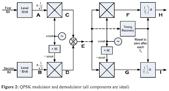
Assume that this sequence, continuously repeated, is applied to the QPSK modulator shown in Figure 2. The corresponding constellation is shown in Figure 3. Both bits of each dibit are presented simultaneously to the product modulators and these levels are maintained for the duration of the symbol time T s. This is coherent QPSK, with exactly two cycles of carrier occurring during each symbol. The carrier frequency is 1600Hz.
Tasks
i. Write a computer simulation to calculate the waveforms at points A, B, C, D, E, F, G, H, I on the modulator/demodulator block diagrams (Figure 1) and print or plot these one beneath the other in their correct time relationship. Ensure that they are labelled unambiguously with the appropriate letter. In the case of the integrator outputs (H and I) the instantaneous waveforms are required. These will resemble figure 2.8 in Study Book 1.
NB: You may not use a commercial simulation package, or a MATLAB toolbox.
ii. Use a Fast Fourier Transform (FFT) algorithm to calculate the print or plot the frequency spectrum of the repeated transmitted modulated carrier E. Use as many repetitions of the waveform as possible.