Question 1: State with reasons, whether the given statements are true or false.
a) 50 µF capacitor and 50 µH inductor provide the same impedance at 100 Hz frequency.
b) Maximum power transfer theorem holds good only for resistive load circuits.
c) Doping decreases the band gap of a semiconductor.
d) Application of bypass capacitor in a CE amplifier disturbs its DC operating point.
e) Oscillator circuit can be built by using a network of only resistors.
f) CMRR finds out the smallest amplitude of the input signal that an op-amp can faithfully amplify.
g) All the fixed voltage regulator ICs are protected against the drop in the input voltage below a set limit.
h) IC380 can be used just to amplify the signal 50 times.
i) Binary code can be employed to represent just the positive integer numbers.
j) D-flip flop and D-latch are one and the same.
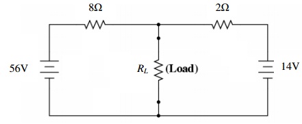
Question 2: Obtain the Thevenin and Norton equivalents of circuit shown in figure below:
Question 3:
a) A band stop filter attenuates a narrow band of frequencies and permits to pass all other frequency signals. Draw a schematic of a band pass filter made of combination of low and high pass filters. As well plot the attenuation characteristics of such filters to result into band stop action.
b) List out any five kinds of semiconductor diode you have came across all along with one application of each.
Question 4:
a) Draw the circuit of push-pull amplifier. Describe how it gives highly efficient operation with very low distortion.
b) Draw the circuit diagram of tuned collector oscillator. Describe how positive feedback is produced in this circuit.
Question 5:
a) Compare the performance of half-wave and centre tapped full wave amplifier on the basis of diode ratings, DC current output, ripple factor, rectification efficiency and cost.
b) Describe the working of capacitor filter. What is the effect of raise in capacitance value on the time constant and ripple in the load current?
Question 6:
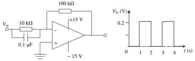
a) Draw the output waveform for the circuit shown in figure below for the Vin shown in figure below.
b) Compute the minimum slew rate of an op-amp required to obtain the output of ± 10V triangular wave at 1 MHz frequency.
Question 7:
a) Design a variable voltage regulator for + 10 to + 15 V output by using IC317.
b) Transform 0001011001010000 into its hexadecimal code. Divide it by 1000012. Express the result in its octal equivalent.
Question 8:
a) Obtain the MSP expression for
Y = AB‾ + A‾B + AB
Write its truth table. Which logic gate is represented by this expression?
b) Design a Mod 11 counter.
Question 9:
a) In a 6 bit DAC the output voltage for 010000 input is 3.2V. What is the maximum output voltage of this DAC? What is the step size and percentage resolution?
b) Name any five main sub-systems of a CRO and briefly elucidate the application of each of them in the functioning of CRO.