Project: Design a single output active load differential amplifier for 4V peak-to-peak output swing and phase margins of 60o or greater. Use Vdd = 5V.
SPECIFICATIONS:
An amplifier is to be realized that meets the following specifications:
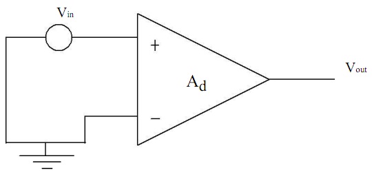
1) A differential to single-ended voltage gain Ad > 96dB
2) An output voltage swing: >4V peak-to-peak.
3) A unity gain bandwidth fu > 90MHz.
4) Phase margin PM > 60o
5) Common mode input range > 3V
6) DC power dissipation < 0.4mW
7) You can use only one voltage source Vdd (5V) for your design. Do not use any resistor.
Device Models:
Technology: AMI 0.6u 5V CMOS, Power supply: VDD = 5 V
Transistor models:
nMOS:
/home/ncsu-cdk-1.6.0.beta/models/hspice/standalone/ami06N.m
TOX = 1.41E-8 m
U0 = 533.6953445 cm^2/V-s
VTH0 = 0.7086 V
pMOS:
/home/ncsu-cdk-1.6.0.beta/models/hspice/standalone/ami06P.m
TOX = 1.41E-8 m
U0 = 202.4540953 cm^2/V-s
VTH0 = -0.9179952V
k’ = UO ⋅ COX , COX = εOX / TOX, εOX = 3.5E-13 F/cm
PROCEDURE:
A reasonable procedure to use in this design is as follows:
1) Choose the basic building blocks and topology.
2) Use a combination of hand calculations and simulations of simplified circuits (e.g. use an ideal current source with a parallel resistor instead of a MOS current source) to find your approximate circuit performance.
3) Loop back to 2, but choose other topologies and circuit blocks and see how the results compare. (Exceeding the basic specifications on gain, output swing, and bandwidth does not earn extra credit).
4) Optimize the device sizes and bias currents to minimize area and power of the most promising circuit.
5) Finish circuit design of current sources and do a complete set of final simulations.
PROJECT REPORT GUIDELINES:
The report must be comprehensive, clear and short. The report must be typed. Maximum pages: 10 pages (11 point or larger font, 1 & 1/2 line spacing or larger).
Here is an outline of what the report muat contain with maximum page limits:
A) A brief introduction of the design problem and a statement of the design goals.
B) Show how you approached the design specifications and how you computed the MOSFET widths and lengths. Describe your design insights and tradeoffs in sizing the transistors.
C) A circuit schematic exhibiting all the MOSFET widths and lengths and SPICE node numbers.
D) A table of all pertinent computed and simulated results. Whenever possible, the simulated values must be compared to the computed values and percentage errors given.
E) Discussion of your results and conclusions regarding the design. Describe and illustrate the differences between your calculated and simulated results. If you failed to meet up one or more of the design criteria, describewhy. Propose how your design could be further improved. Comment on any other features of the design as you see fit.